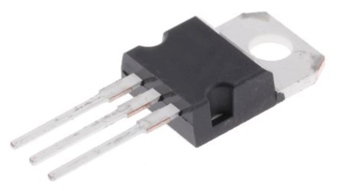
onsemi N型沟道 增强型 功率 MOSFET, Vds=650 V, 19 A, TO-220, 通孔安装, 3引脚, SUPERFET III系列
- RS 库存编号:
- 178-4676P
- 制造商零件编号:
- FCP165N65S3
- 制造商:
- onsemi

可享批量折扣
查看批量定价选项小计 15 件 (按管提供)*
RMB448.62
(不含税)
RMB506.94
(含税)
最后的 RS 库存
- 最终 685 个,准备发货
单位 | 每单位 |
|---|---|
| 15 - 20 | RMB29.908 |
| 25 + | RMB29.014 |
* 参考价格
- RS 库存编号:
- 178-4676P
- 制造商零件编号:
- FCP165N65S3
- 制造商:
- onsemi
产品技术参数
产品技术参数资料
法例与合规
产品详细信息
通过选择一个或多个属性来查找类似产品。
选择全部 | 属性 | 值 |
|---|---|---|
| 品牌 | onsemi | |
| 槽架类型 | N型 | |
| 产品类型 | 功率 MOSFET | |
| 最大连续漏极电流 Id | 19A | |
| 最大漏源电压 Vd | 650V | |
| 包装类型 | TO-220 | |
| 系列 | SUPERFET III | |
| 安装类型 | 通孔 | |
| 引脚数目 | 3 | |
| 最大漏源电阻 Rd | 165mΩ | |
| 通道模式 | 增强 | |
| 最低工作温度 | -55°C | |
| 典型栅极电荷 Qg @ Vgs | 39nC | |
| 正向电压 Vf | 1.2V | |
| 最大功耗 Pd | 154W | |
| 最高工作温度 | 150°C | |
| 高度 | 16.3mm | |
| 长度 | 10.67mm | |
| 标准/认证 | RoHS, Pb-Free, Halide Free | |
| 汽车标准 | 否 | |
| 选择全部 | ||
|---|---|---|
品牌 onsemi | ||
槽架类型 N型 | ||
产品类型 功率 MOSFET | ||
最大连续漏极电流 Id 19A | ||
最大漏源电压 Vd 650V | ||
包装类型 TO-220 | ||
系列 SUPERFET III | ||
安装类型 通孔 | ||
引脚数目 3 | ||
最大漏源电阻 Rd 165mΩ | ||
通道模式 增强 | ||
最低工作温度 -55°C | ||
典型栅极电荷 Qg @ Vgs 39nC | ||
正向电压 Vf 1.2V | ||
最大功耗 Pd 154W | ||
最高工作温度 150°C | ||
高度 16.3mm | ||
长度 10.67mm | ||
标准/认证 RoHS, Pb-Free, Halide Free | ||
汽车标准 否 | ||
- COO (Country of Origin):
- CN
SUPERFET III MOSFET is ON Semiconductor’s brand−new high voltage super−junction (SJ) MOSFET family that is utilizing charge balance technology for outstanding low on−resistance and lower gate charge performance. This advanced technology is tailored to minimize conduction loss, provide superior switching performance, and withstand extreme dv/dt rate.
700 V @ TJ = 150 °C
Ultra Low Gate Charge (Typ. Qg = 39 nC)
Low Effective Output Capacitance (Typ. Coss(eff.) = 341 pF)
Internal Gate Resistance: 4.6 Ω
Optimized Capacitance
Typ. RDS(on) = 140 mΩ
Benefits:
Higher system reliability at low temperature operation
Lower switching loss
Lower switching loss
Lower peak Vds and lower Vgs oscillation
Lower peak Vds and lower Vgs oscillation
Applications:
Computing
Consumer
Industrial
End Products:
Notebook / Desktop computer
Game Console
Telecom / Server
LCD / LED TV
LED Lighting / Ballast
Adapter